Circuit Technology Center
 
No. 6.3
Component Modifications and Additions

OUTLINE
This procedure covers the general guidelines for modifications that involve adding components.

REFERENCES
PROCEDURE REFERENCE
CTC 7721 2.1 Handling Electronic Assemblies
CTC 7721 2.2 Cleaning
CTC 7721 2.5 Baking and Preheating
CTC 7721 2.7 Epoxy Mixing and Handling
CTC 7721 6.1 Jumper Wires


TOOLS & MATERIALS
Cleaner
Cleaning Wipes
Flux
Microscope System
Soldering Iron with Tips
Solder


GENERAL RULES
  1. Added components may need to be secured with adhesive, or by other means, if the component leads or component body would be subjected to mechanical stress.


  2. Leads of added components should not be inserted into plated holes occupied by another component lead.


  3. Added components placed on the circuit board surface should be placed on the component side of the assembly or circuit board unless otherwise specified.


  4. Added components shall not be raised above the board surface beyond allowable dimensions.


  5. Added components shall not cover over pads or vias used as test points.


  6. Added components shall not cover other component foot prints unless the layout of the assembly prohibits mounting in other areas.


  7. Added component leads may require insulation to avoid contact with component body or other conductors.


  8. Removal of existing solder from a connection point may be necessary to avoid bridging, or excess solder, in the final connection.


  9. Consider design limitations and product use environments when stacking components.


  10. Do not exceed minimum component lead bend radius.


  11. When possible, component identification marking shall be legible.

PROCEDURE
  1. When required, form the component leads and clean the area.


  2. When required, secure the component in place by bending leads or other mechanical means.


  3. Apply flux to the joint.


  4. Place the soldering iron tip at the connection between both leads. Apply a small amount of solder at the connection of soldering iron tip and lead to form a solder bridge.


  5. Immediately feed solder into the joint from the side opposite from the soldering iron tip until the proper fillet is achieved. Remove the solder and iron simultaneously.


  6. When required, clean the flux residue.


  7. Inspect.
 
Solutions Across the Board TM

Product Class:  R/F/W/C
Skill Level:  Advanced
Conformance Level:  N/A
Revision:  A
Revision Date:  Feb 1, 2001
Repair Service Charge

  
Component Modifications
and Additions


Component Modifications and Additions Figures


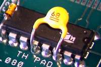
Figure 1: Radial lead component soldered to through hole component leads. Note: Leads of the radial component should not need to be inserted into the plated holes.

 
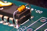
Figure 2: Axial lead component soldered to through hole component leads. Note: Leads of axial component should not be inserted into the plated holes.


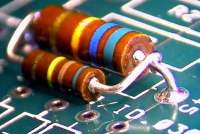
Figure 3: Axial lead component soldered to adjacent axial lead component. Note: Added component may be stacked vertically or horizontally.

 
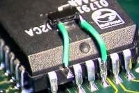
Figure 4: Chip component soldered to surface mount component using jumper wires. Note: One lead of surface mount component is shown lifted.


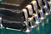
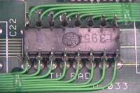
Figure 5: DIP component stacked and soldered onto another DIP component. One lead shown clipped. Note: Leads of added component should not be inserted into the plated holes.

 
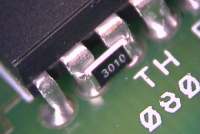
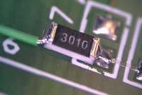
Figure 6: Chip cap bridging adjacent leads.


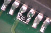
Figure 7: Chip component bridging leads of surface mount component.

 
Figure 8: Chip component stacked onto another chip component.


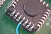
Figure 9: Surface mount component mounted upside down with jumper wires attached. Note: One lead is bent outward.

 
Figure 10: DIP Component mounted upside down with jumper wires attached.


Figure 11: Chip component mounted to one pad only.

 
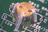
Figure 12: Radial lead component mounted upside down. Note: Insulate leads to avoid contact with component body.
 
 
Home · Services · Guidebook · Products · Training · Top

Circuit Technology Center, Inc.