No. 6.2.1
Jumper Wires, BGA Components, Circuit Track Method
OUTLINE
This method is used to change a circuit path at a BGA site for engineering
changes or modifications.
NOTE
This procedure requires precision milling equipment and highly trained
technicians.
CAUTION
This procedure is not applicable for "via in pad" applications.
| ACCEPTABILITY REFERENCES |
| IPC-A-600 |
2.0 |
Externally Observable Characteristics |
| IPC-A-610 |
11.0 |
Discrete Wiring |
| |
| PROCEDURE REFERENCE |
| CTC 7721 |
2.1 |
Handling Electronic Assemblies |
| CTC 7721 |
2.2 |
Cleaning |
| CTC 7721 |
2.5 |
Baking and Preheating |
| CTC 7721 |
2.7 |
Epoxy Mixing and Handling |
| CTC 7721 |
4.2.1 |
Conductor Repair, Foil
Jumper, Epoxy Method |
| CTC 7721 |
4.4.3 |
Surface Mount, BGA Pad
Repair, Film Adhesive Method. |
| CTC 7721 |
6.1 |
Jumper Wires |
| CTC 7721 |
8.5.2 |
Profile Development, BGA Comp., Hot Gas/Air Method |
| CTC 7721 |
8.5.3 |
Component Replacement, PBGA Comp., Hot Gas/Air Method |
| CTC 7721 |
8.5.4 |
Component Replacement, CBGA Comp., Hot Gas/Air Method |
| IPC 7721 |
6.2.1 |
Jumper Wires, BGA Components, Circuit Track Method |
TOOLS & MATERIALS
BGA Pad Repair Kit
Bonding Iron
Bonding Tips
Bonding System
Circuit Frames, BGA Pads
Circuit Tracks
Cleaner
End Mills
Epoxy
Flux, Liquid
Heat Lamp
Knife
Microscope
Milling System
Oven
Precision Drill System
Scraper
Solder
Soldering Iron
Tape, Kapton
Tweezers
Wipes
PROCEDURE
- Clean the area.
- Remove the BGA component if installed, remove excess solder from the pads,
and clean and inspect the site using standard BGA rework equipment.
- Cut the short conductor (dog bone) connecting the BGA pad to the connecting
via using a Precision Drill System or milling machine and appropriate size end
mill. (See Figure 1 and 6).
- Remove the existing BGA pad. Apply heat from a soldering iron if needed.
(See Figure 2)
- Use a milling machine to mill a shallow groove in the board surface from the
BGA pad area to the perimeter of the BGA site. Tight spacing may restrict the
width of the channel to 0.25 mm (.010") or less. Use a carbide end mill
approximately0.050 mm (.002") wider than the new connecting circuit. (See
Figure 3).
- Bond a replacement BGA pad in place using a bonding system. (See Procedure
4.7.3). The new BGA pad must have a tail that will align with the circuit track
to be added next. (See Figure 4).
- Select a Circuit Track to match the width and thickness of the circuit to be
replaced. Cut a length approximately as needed. The Circuit Track should overlap
the BGA tail section a minimum of 2 times the circuit width. See Table 1.
Table 1
Common Circuit Track Sizes
| Part No. |
Thickness |
Width |
| 115-5204 |
.002" |
.004" |
| 115-5206 |
.002" |
.006" |
| 115-5208 |
.002" |
.008" |
| 115-5210 |
.002" |
.010" |
| 115-5312 |
.003" |
.120" |
| 115-5315 |
.003" |
.015" |
| 115-5520 |
.005" |
.020" |
| 115-5530 |
.005" |
.030" |
- Gently abrade the top and bottom of the new Circuit Track with the buffer to
remove any oxidation and clean.
NOTE
If needed, the ends of the Circuit Track may be tinned with solder prior to lap
soldering in place.
- Position this new Circuit Track along the milled groove. The Circuit Track
should overlap the existing circuit a minimum of 2 times the circuit width. (See
Figure 4).
- Apply a small amount of liquid flux to the overlap joint.
- Lap solder the Circuit Track to the BGA tail section using solder and a
soldering iron. Make sure the new circuit is properly aligned.
- Solder one end of a fine gauge wire to the end of the extending circuit.
(The opposite end of the wire will be soldered later.) (See Figure 5).
- Clean the area.
- Mix epoxy. If desired, add color agent to the mixed epoxy to match the circuit
board color.
- Coat the top and sides of the replaced circuit with epoxy. The epoxy bonds
the new circuit to the base board material and insulates the circuit. (See
Figure 5).
- Cure the epoxy per Procedure 2.7 Epoxy Mixing and Handling.
CAUTION
Some components may be sensitive to high temperature.
- Clean the board as required.
- Install new BGA per applicable procedures.
- Route and terminate the other end of the jumper wire.
EVALUATION
- Visual examination for alignment and overlap of new circuit.
- Visual examination of epoxy coating for texture and color match.
- Electrical tests as applicable.
|
|
|
Solutions Across the Board
TM
|
|
|
|
Product Class: R/F
Skill Level: Expert
Conformance Level: Medium
Revision: B
Revision Date: Jul 7, 2000
Repair Service Charge
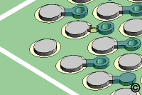 Figure 1: Cut the connection to the via using a Precision Drill System.
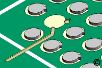 Figure 2: Remove the BGA pad and mill a shallow channel into the solder mask surface.
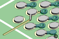 Figure 3: Bond a new BGA pad in place.
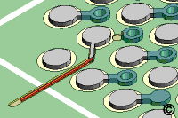 Figure 4: Solder a copper circuit track to the tail extending from the new BGA pad.
 Figure 5: Solder a wire to the Circuit Track and overcoat with epoxy.
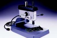 Figure 6: Precision Drill System used to cut the connection from the BGA pad to the via.
|
Tricks of the Trade
A unique repair method pioneered at Circuit Technology Center.
Call for more information.
|
|
|
