No. 4.2.7
Conductor Repair, Surface Plane, Film Adhesive Method
OUTLINE
This method is used to repair damaged circuit surface planes. The damaged areas are repaired with dry film epoxy, adhesive backed
copper foil disks. They are bonded to the circuit board surface using a bonding press or bonding iron.
CAUTION
It is essential that the board surface be extremely smooth and flat. If the base board is damaged see appropriate procedure.
TOOLS & MATERIALS
Abrasive Pad
Adhesive Backed Circuit Material
Bonding Iron
Bonding Tips
Bonding System
Cleaner
Cotton Tipped Applicator
Desolder Braid
End Mills
Electric/Hand Eraser
Epoxy
Flux, Liquid
Gray Eraser Stick
Green Eraser Stick
Knife
Microscope
Oven
Precision Drill/Milling System
Scraper
Solder
Soldering Iron
Surface Mount Pad Repair Kit
Tape, Kapton
Tweezers
Wipes
PROCEDURE
- Clean the area.
- Secure the circuit to a Precision Drill/Milling System with a microscope available for viewing. Use an end mill slightly larger than the void in
the surface plane and make a counter bore through the surface plane only. Do not mill into the laminate material, you may expose inner
layer circuits.
NOTE
Several adjacent counter bores may be required to fill larger areas.
- Clean the area with solvent.
- The area for the new Adhesive Backed Disk on the board surface must be smooth and flat. If internal fibers of the board are exposedor there are deep scratches in the surface they should be repaired. Refer to appropriate procedure.
- Select a replacement adhesive backed disk that matches the size of the end mill used to make the counter bore.
NOTE
The thickness should be selected to meet the requirements of the circuit board surface plane thickness.
- With the adhesive backed disk positioned film side up, carefully scrape off the adhesive film from the outer 0.005” of the disk diameter.
- Position the adhesive backed disk, film side down. Place a piece of Kapton tape over adhesive backed disk, position the adhesive backed disk into the counter bore. Press the adhesive backed disk into position. (See Figure 2).
- Select a bonding tip with a shape to match the shape of the adhesive backed disk.
NOTE
The bonding tip should be as small as possible but should completely cover the entire surface of the adhesive backed disk.
- Position the circuit board so that it is flat and stable. Gently place the hot bonding tip onto the Kapton tape covering the adhesive backed disk. Apply pressure and heat as recommended in the manual of the Repair
System or Repair Kit for 5 seconds to tack the adhesive backed disk in
place. Carefully peel off the tape. (See Figure 3).
- Gently place the hot bonding tip directly onto the new adhesive backed disk. Apply pressure and heat as recommended in the manual of the Repair
System or Repair Kit for an additional 30 seconds to fully bond the
new adhesive backed disk. The new adhesive backed disk is fully cured. Carefully clean the area and inspect
the new adhesive backed disk for alignment.
NOTE
Several adjacent counter bores may be required to fill larger areas.
- Using flux and solder, carefully add a small amount of solder to a soldering iron with a “Blade” shaped tip, and flow solder over the repaired area.
- Using the “Blade” shaped soldering tip and desolder braid, remove any excess solder
- Clean the area.
- Using the Electric/Hand Eraser, clean and buff the soldered area to blend the repair to the circuit surface.
- Using Kapton tape, mask off an area larger than the repaired area.
- Using the abrasive pad, “lightly” buff the masked area to further blend the repair to the circuit surface as necessary. (See figure 4)
- Clean the area.
FINAL FINISH
- Blend the surface type using an appropriate buffing material, such as:
Scotch Bright, Kim Wipes, or Cotton Tipped Applicator.
- Matte and semi-gloss surfaces may require light abrasion in order to blend
to original surface finish type. High gloss will require polishing with a Kim
Wipe or a Cotton Tipped Applicator chucked in a Micro Drill System.
- Remove any loose particles as necessary and clean the area.
EVALUATION
- Visual examination
- Electrical tests as applicable.
|
|
|
Solutions Across the Board
TM
|
|
|
|
Product Class: R
Skill Level: Advanced
Conformance Level: Medium
Revision: B
Revision Date: Mar 28, 2001
Repair Service Charge

Damaged Surface Plane

Figure 1: Milled area to remove damaged foil .

Figure 2: Transplant new foil disk into milled out area.
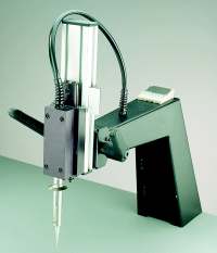
Figure 3: Bond the new adhesive backed disk using a commercially available
Bonding System.

Figure 4: Solder tin the area and blend in.
|
|
|