Circuit Technology Center
 
Circuit Frames

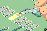
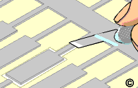
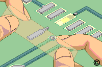
Imagine replacing damaged circuits without the mess of liquid epoxy, with a bond strength equal to the original, on bare or loaded circuit boards -- all in about 30 seconds. Our replacement Circuit Frames with dry-film epoxy backing make this delicate, precise procedure quick and neat. Trim out the circuit you need and bond it to the circuit board surface with a bonding iron or bonding press.

Choose from hundreds of different shapes or let us custom design and fabricate that special shape for you.

Replacing circuits and pads is done in 4 steps.

Step 1 (See Figure 1.)
Evaluate the damaged circuits. If the base material is severely damaged it may have to first be repaired using epoxy. See Epoxy Kits. Remove the defective pad or conductor and scrape off any soldermask from the connecting circuit. Apply liquid flux to the connecting circuit on the board surface and tin with solder.

Step 2 (See Figure 2.)
Select a replacement pad that matches the missing pad. Scrape off the adhesive bonding film from the solder joint area on the back of new pad. Trim out the new pad from the Circuit Frame. Cut from the plated side.

Step 3 (See Figure 3.)
Temporarily place the new pad in position using Kapton tape. Then permanently bond the new pad using the Bonding System or Bonding Iron. Bonding time is only 30 seconds.

Step 4 (See Figure 4.)
If the new conductor has a connecting circuit, apply liquid flux to the lap solder joint connection area and solder the circuit of the new pad to the circuit on the printed circuit board surface. If desired, apply epoxy to the lap solder joint connection.

Material Specifications
Frame Size: 2.25" x 1.50" (57 x 38 mm)
Base Material: Rolled annealed copper foil .0014" (.036 mm) thick
Adhesive Backing: Phenolic Butral film adhesive .0018" (.046 mm) thick
Bonding Temperature: 475°F ± 25°F (246°C ± 14°C)
Bonding Time: 30 seconds
Bonding Load: See Calibration Settings below
Peel Strength: Minimum 8 lbs/inch (1.43 kg/cm) after cure to FR-4 material
Shelf Life: 6 months minimum.

Plating Specifications
Tin - Tin/Lead: .001" (.0254 mm) 60/40 tin/lead minimum
Gold - Nickel/Gold:: .000050" (.00127 mm) gold over .000100" (.00254 mm) nickel minimum
 
Solutions Across the Board TM

Ordering Information

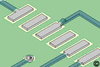
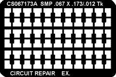
Sample replacement surface mount pads.


1. Remove the damaged pads and prepare the area.


2. Select a replacement pad and trim it out from the Circuit Frame.


3. Place the pad in position using tape and bond in place.


4. Complete the connection to the existing circuit.

Circuit Frame Table
Part Number Surface Mount Pad Frames - Price $33.00 each Plating Bonding Tip Load
CS004085AT Surface Mount Pads .004" x .085" (0.10 mm x .20 mm) Tin 115-2304 A
CS012060AT Surface Mount Pads .012" x .060" (0.30 mm x 1.52 mm) Tin 115-2302 A
CS012100AT Surface Mount Pads .012" x .100" (0.30 mm x 2.54 mm) Tin 115-2308 * A
CS020028AT Surface Mount Pads .020" x .028" (0.508 mm x 0.711 mm) Tin 115-2310 A
CS025080AT Surface Mount Pads .025" x .080" (0.63 mm x 2.03 mm) Tin 115-2304 B
CS025080BT Surface Mount Pads .025" x .080" (0.63 mm x 2.03 mm) Tin 115-2304 B
CS028050AT Surface Mount Pads .028" x .050" (0.71 mm x 1.27 mm) Tin 115-2312 * A
CS028185AT Surface Mount Pads .028" x .185" (0.71 mm x 4.70 mm) Tin 115-2314 C
CS030055AT Surface Mount Pads .030" x .055" (0.76 mm x 1.40 mm) Tin 115-2312 * B
CS034030AT Surface Mount Pads .034" x .030" (0.86 mm x 0.76 mm) Tin 115-2310 A
CS038090AT Surface Mount Pads .038" x .090" (.97 mm x 2.28 mm) Tin 115-2308 B
CS040070AT Surface Mount Pads .040" x .070" (1.01 mm x 1.77 mm) Tin 115-2312 B
CS040110AT Surface Mount Pads .040" x .110" (1.01 mm x 2.80 mm) Tin 115-2308 B
CS045110AT Surface Mount Pads .045" x .110"(1.14 mm x 2.80 mm) Tin 115-2308 B
CS046106AT Surface Mount Pads .046" x .106" (1.17 mm x 2.70 mm) Tin 115-2308 B
CS048068AT Surface Mount Pads .048" x .068" (1.22 mm x 1.73 mm) Tin 115-2312 B
CS050050AT Surface Mount Pads .050" x .050" (1.27 mm x 1.27 mm) Tin 115-2310 B
CS051087AT Surface Mount Pads .051" x .087" (1.30 mm x 2.21 mm) Tin 115-2204 B
CS060080AT Surface Mount Pads .060" x .080" (1.52 mm x 2.03 mm) Tin 115-2312 B
CS065055AT Surface Mount Pads .065" x .055" (1.65 mm x 1.40 mm) Tin 115-2312 B
CS065095AT Surface Mount Pads .065" x .095" (1.65 mm x 2.41 mm) Tin 115-2316 C
CS067173AT Surface Mount Pads .067" x .173" (1.70 mm x 4.39 mm) Tin 115-2318 * D
CS071106AT Surface Mount Pads .071" x .106" (1.80 mm x 2.69 mm) Tin 115-2316 C
CS090095AT Surface Mount Pads .090" x .095" (2.28 mm x 2.41 mm) Tin 115-2320 C
CS090100AT Surface Mount Pads .090" x .100" (2.28 mm x 2.54 mm) Tin 115-2206 C
CS095095AT Surface Mount Pads .095" x .095" (2.41 mm x 2.41 mm) Tin 115-2320 C
CS130177AT Surface Mount Pads .130" x .177" (3.30 mm x 4.42 mm) Tin Custom E
         
Part Number Ball Grid Array Pad Frames - Price $33.00 each Plating Bonding Tip Load
CS015020AT BGA Pads .015"/.020" (0.38 mm x 0.50 mm) Diameter Tin 115-2201 A
CS020025AT BGA Pads .020"/.025" (0.38 mm x 0.63 mm) Tin 115-2312 A
CS025035AT BGA Pads .025"/.035" (0.63 mm/.89 mm) Diameter Tin 115-2202 A
CS051063AT BGA Pads .051'/.063" (1.29 mm/1.60 mm) Diameter Tin 115-2204 B
         
Part Number Conductor Frames - Price $33.00 each Plating Bonding Tip Load
CT006015AT Conductor Tracks .006"/.015" (0.15 mm/0.38 mm) Tin 115-2314 * **
CT006025AT Conductor Tracks .006"/.025" (0.15 mm/0.63 mm) Tin 115-2314 **
         
Part Number Gold Edge Contact Frames - Price $49.00 each Plating Bonding Tip Load
CC035080AG Gold Edge Contacts .035" x .080" (0.89 mm x 2.03 mm) Gold 115-2312 * B
CC038255AG Gold Edge Contacts .038" x .250" (0.97mm x 6.35 mm) Gold 115-2314 * C
CC050060AG Gold Edge Contacts .050"/.060" (1.27 mm/1.52 mm) Gold 115-2314 F
CC050300AG Gold Edge Contacts .050" x .300" (1.27 mm x 7.62 mm) Gold 115-2314 * E
CC070080AG Gold Edge Contacts .070"/.080" (1.78 mm/2.03 mm) Gold 115-2318 F
CC070210AG Gold Edge Contacts .070" x .210" (1.78 mm x 5.33 mm) Gold 115-2318 F
CC076190AG Gold Edge Contacts .076" x .190" (1.93 mm x 4.83 mm) Gold 115-2318 * D
CC085360AT Gold Edge Contacts .085" x .360" (2.16 mm x 9.14 mm) Gold 115-2318 F
CC090300AG Gold Edge Contacts .090" x .300" (2.28 mm x 7.62 mm) Gold 115-2322 F
CC094230AG Gold Edge Contacts .094" x .230" (2.39 mm x 5.84 mm) Gold 115-2322 D
         
Part Number Land Frames - Price $33.00 each Plating Bonding Tip Load
CP050060AT Lands .050"/.060" (1.27 mm/1.52 mm) Tin 115-2202 C
CP067267AT Lands .067" x .267" (1.70 mm/6.78 mm) Tin 115-2318 * E
CP070080AT Lands .070"/.080" (1.78 mm/2.03 mm) Tin 115-2204 C
CP090100AT Lands .090"/.100" (2.28 mm/2.54 mm) Tin 115-2206 D
CP090100BT Lands .090" x .100" (2.28 mm x 2.54 mm) Tin 115-2206 C
CP140210AT Lands .142" ID x 210" OD (3.60 mm ID x 5.33 mm OD) Tin Custom F
CP156097AT Lands .156 OD x .097 ID (3.96 mm OD x 2.46 mm ID) Tin Custom F
CP250125AT Lands .250" OD x .125" ID (6.35 mm OD x 3.18 mm ID) Tin Custom F
         
Part Number Variety Frames - Price $33.00 each Plating Bonding Tip Load
CFV002AT Variety Tin Variety **
CVAR0001AT Variety .010" Track (0.254 mm) Tin Variety **
CBLANKAT Circuit Frame, Blank Tin Variety **

Bonding Tip
Bonding Tip listing in the above table is the recommended Bonding Tip to use with the particular Circuit Frame.
* Indicates that the closest size Bonding Tip has been listed, a custom size Bonding Tip may be required.
** Indicates that Bonding Loads will vary depending on the particular circuit selected from the Circuit Frame.

Manual Bonding Load Table
Circuit Surface Area Load Setting Hand Bonding Setting
Up to .002 in2
Up to 1.29 mm2
4 oz.
( 113 grams)
A A - Very Light Load
Approximately equal to the weight of the Bonding Iron.
.002 in2 to .005 in2
1.30 mm2 to 3.22 mm2
8 oz.
( 227 grams)
B B - Light Load
Slightly less than twice the weight of the Bonding Iron.
.005 in2 to .010 in2
3.22 mm2 to 6.45 mm2
12 oz
( 340 grams)
C C - Light Load
Slightly greater than twice the weight of the Bonding Iron.
.010 in2 to .015 in2
6.45 mm2 to 9.67 mm2
24 oz.
( 680 grams)
D D - Medium Load
Approximately half the resting weight of your arm.
.015 in2 to .025 in2
9.67 mm2 to 16.13 mm2
32 oz.
( 907 grams)
E E - Firm Load
Slightly less than the resting weight of your arm.
.025 in2 and greater
16.13 mm2 and greater
48 oz.
(1361 grams)
F F - Firm Load
Approximately equal to the resting weight of your arm.

Bonding Loads
To obtain the maximum bond of the Circuit Frame to the circuit board surface, the proper Bonding Tip temperature, Bonding Tip time, and Bonding Tip load are required. The Bonding Load is based upon the approximate surface area of the replacement circuit. Bonding Irons are included in several repair kits or available separately.

Settings A through F are listed on the Calibration Slide of the Circuit Technology Center Bonding System.
 
 
Home · Services · Guidebook · Products · Training · Top

Circuit Technology Center, Inc.


Send Comments To: info@circuittechctr.com
©2000 Circuit Technology Center. All rights reserved.