No. 4.2.6
Conductor Repair, Inner Layer Method
OUTLINE
This method is used to replace damaged or missing circuits on internal layers of
multilayer circuit boards.
CAUTION
The circuit widths, spacing and current carrying capacity must not be reduced
below allowable tolerances.
CAUTION
The overlap joint used in this method may cause problems with high frequency
circuitry.
CAUTION
This procedure is complicated and should be attempted only by properly skilled
repair personnel using the best tools and equipment.
TOOLS & MATERIALS
Ball Mills
Buffer
Circuit Tracks
Cleaner
Color Agent
Epoxy
Flux, Liquid
Knife
Micro-Drill System
Microscope
Oven
Scraper
Soldering Iron
Solder
Tape, Kapton
Wipes
PROCEDURE
- Locate and determine the coordinates where the repair is to be made. Use
films or master drawings of the board as needed.
NOTE
Obtain as much information as possible on the conductive and non-conductive
layers prior to starting the procedure.
- Remove components from the immediate area if necessary and clean the area.
- Use the microscope and Micro-Drill System and cut through the base material,
one layer at a time, until the desired inner layer has been reached. (See Figure
1 and 2).
CAUTION
Great care should be taken to prevent further damage to internal circuits.
- Each internal circuit should have a flat section exposed to allow the new
circuit to be soldered in place. (See Figure 3).
NOTE
To reduce damage to the internal circuit, complete the final exposure of the
internal circuit using a knife. (See Figure 3).
- Remove all loose material. Clean the area.
- Apply a small amount of liquid flux to the ends of the internal circuit. Tin
the exposed end of each circuit using solder and a soldering iron.
- Clean the area.
- Select a Circuit Track to match the width and thickness of the circuit to be
replaced. Cut a length approximately as needed. The Circuit Track should overlap
the existing circuit a minimum of 2 times the circuit width.
- Gently abrade the top and bottom of the Circuit Track with the buffer to
remove any protective coating and clean.
NOTE
If needed, the ends of the Circuit Track may be tinned with solder prior to lap
soldering in place.
- Place the Circuit Track in position. The Circuit Track should overlap the
existing circuit a minimum of 2 times the circuit width. (See Figure 4).
NOTE
If spacing is critical or the circuit Board uses high frequency circuits, bevel the
joint. (See Figure 5).
CAUTION
This bevel joint method may cause problems with circuit Boards exposed to extreme
temperature fluctuations.
- Apply a small amount of liquid flux to the overlap joint.
- Lap solder the Circuit Track to the exposed internal circuit using solder
and a soldering iron. Make sure the new circuit is properly aligned.
- Clean the area.
NOTE
The circuit Board may be preheated prior to filling the area with epoxy. A preheated
PC Board will allow the epoxy to easily flow and level out. Epoxy applied to an
unheated circuit board may settle below the circuit board surface as the epoxy cures.
- Mix epoxy. If desired, add color agent to the mixed epoxy to match the circuit
board color.
- Coat the top and sides of the replaced circuit with epoxy. The epoxy bonds
the new circuit to the base board material and insulates the circuit. Continue
adding epoxy up to the top surface of the circuit board or to the height of the next
internal circuit. (See Figure 6).
NOTE
A slight overfill of epoxy may be desired to allow for shrinkage when the epoxy
cures.
- Cure the epoxy per Procedure 2.7 Epoxy Mixing and Handling.
CAUTION
Some components may be sensitive to high temperature.
- Add additional Circuit Tracks if needed and coat with additional epoxy.
- Continue completing all layers until the top surface of the circuit board is
reached. (See Figure 7).
- Clean the board as required.
- Apply surface coating to match prior coating as required.
EVALUATION
- Visual examination for alignment and overlap of new circuit.
- Visual examination of epoxy coating for texture and color match.
- Electrical tests as applicable.
|


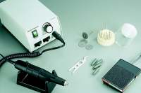
 Figure 3: Remove the remaining board material covering the internal circuit
using the knife.
Figure 3: Remove the remaining board material covering the internal circuit
using the knife.


